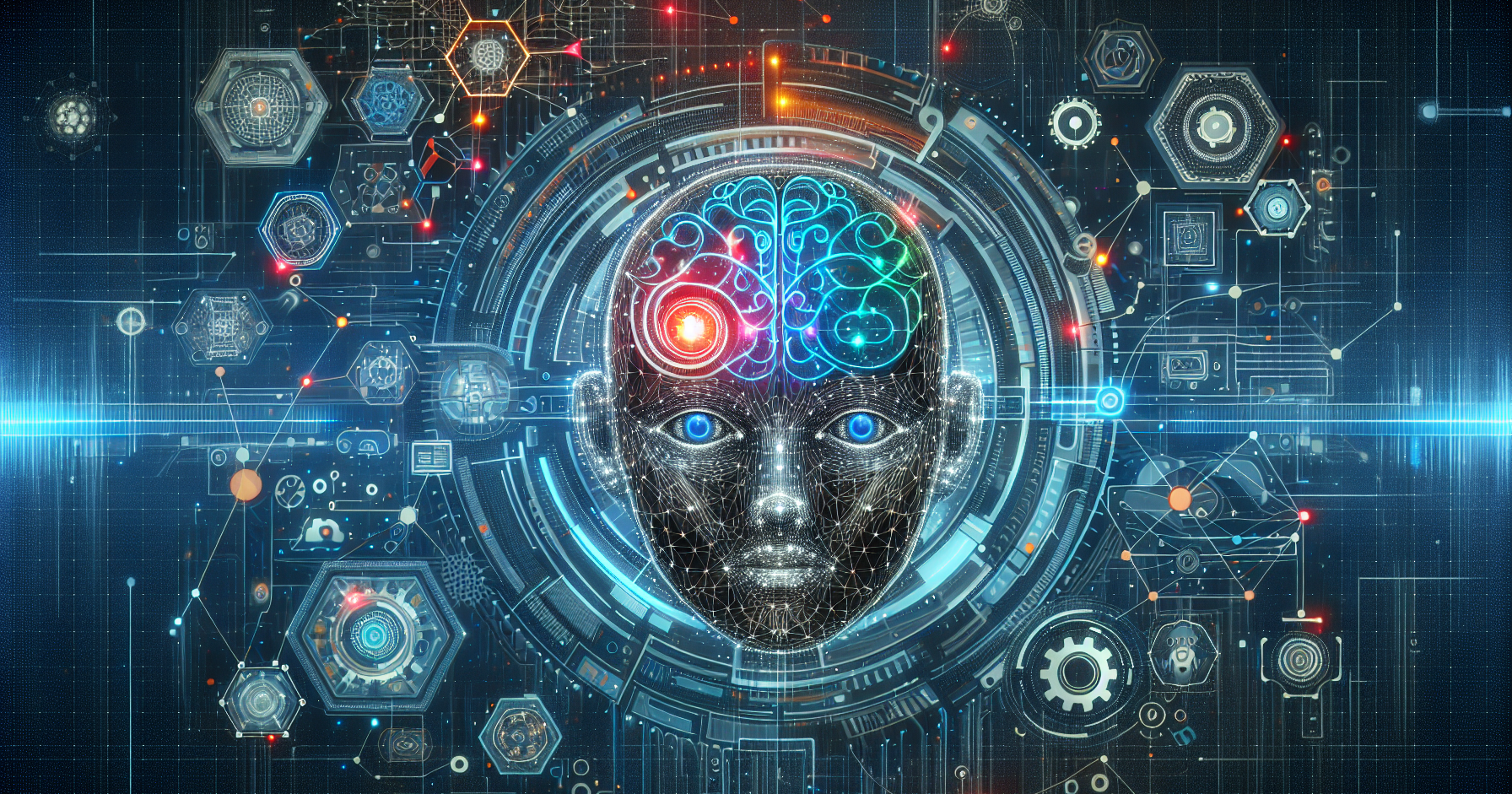
The escalating computational demands of artificial intelligence, particularly in deep learning, present a significant environmental challenge. Training and deploying large-scale AI models, such as those powering generative AI or complex natural language processing, consume vast amounts of electricity, contributing substantially to global carbon emissions. The sheer scale of parameters in models like GPT-3 or AlphaFold, coupled with the iterative nature of training, translates directly into astronomical energy footprints. This necessitates a fundamental shift in how AI hardware is designed and utilized, moving towards more energy-efficient architectures. The imperative for sustainable AI development is not merely an ethical consideration but a strategic necessity for managing operational costs and mitigating the environmental impact of this rapidly expanding technological domain.
Historically, Graphics Processing Units (GPUs) became the workhorse for AI development due to their highly parallel processing capabilities, a design feature initially optimized for rendering complex graphics. Their architecture, with thousands of smaller cores operating simultaneously, proved remarkably adept at the matrix multiplication and convolution operations fundamental to neural networks. However, GPUs are general-purpose processors at their core. While powerful, their flexibility comes at the cost of energy efficiency when performing highly specific, repetitive AI computations. They contain numerous components and instruction sets not always relevant to deep learning, leading to wasted energy. This inherent inefficiency spurred the development of specialized hardware, custom-built from the ground up to accelerate AI workloads with significantly reduced power consumption, marking a pivotal transition from general-purpose to domain-specific computing for AI.
Google’s Tensor Processing Units (TPUs) represent a pioneering effort in this domain. Conceived and developed internally by Google, TPUs were designed specifically to accelerate TensorFlow workloads, Google’s open-source machine learning framework. Their core innovation lies in their architecture, particularly the use of systolic arrays. Unlike traditional CPU or GPU architectures where data is fetched from memory, processed, and then written back, systolic arrays operate more like an assembly line. Data flows through an array of interconnected processing elements, performing calculations (like matrix multiplications) at each stage before passing the results to the next element. This continuous flow minimizes data movement, which is a major energy consumer in conventional architectures, leading to substantial gains in speed and efficiency for tensor operations.
Beyond systolic arrays, TPUs achieve significant energy savings through reduced precision arithmetic. While GPUs often perform calculations using 32-bit (FP32) or 16-bit (FP16) floating-point numbers, TPUs leverage custom formats like bfloat16 (Brain Floating Point, 16-bit) and even 8-bit integers (INT8). Bfloat16 offers a wider dynamic range than FP16, crucial for maintaining accuracy during training, while INT8 is highly effective for inference. Reducing the precision of numbers decreases the amount of data that needs to be stored and processed, directly translating into lower power consumption and faster computation without significant loss of model accuracy in many AI applications. TPUs have evolved through several generations (v1 for inference, v2, v3, v4 for both training and inference), with each iteration delivering exponential improvements in performance per watt, consolidating Google’s leadership in energy-efficient AI infrastructure for services like Google Search, Translate, and AlphaGo.
The success and principles behind TPUs have catalyzed a broader movement towards Neural Processing Units (NPUs). NPUs are a general category of specialized processors designed to accelerate AI and machine learning tasks, particularly neural network operations. While TPUs are Google’s specific implementation, NPUs encompass a diverse range of chips developed by various companies, often tailored for different deployment scenarios, from massive data centers to power-constrained edge devices. These NPUs share common characteristics with TPUs: a focus on highly parallel matrix multiplication, specialized memory hierarchies to reduce latency and power, and support for low-precision arithmetic.
The proliferation of NPUs is particularly critical for Edge AI, where artificial intelligence is deployed directly on devices like smartphones, IoT sensors, autonomous vehicles, and smart appliances rather than relying on cloud-based processing. For these applications, energy efficiency is paramount. Battery life, thermal management, and real-time responsiveness demand processing capabilities that consume minimal power. NPUs from companies like Apple (Neural Engine in A-series chips), Qualcomm (Hexagon DSPs), Intel (various AI accelerators), and even NVIDIA (Tensor Cores within their GPUs, which incorporate NPU-like functionality) are specifically engineered to deliver high inference throughput with extremely low wattage. This enables sophisticated AI features – such as on-device voice assistants, facial recognition, and predictive maintenance – to operate autonomously and efficiently, reducing the need for constant cloud connectivity and its associated energy overhead.
Quantifying the “Green Advantage” of TP
Related Articles

Real-time Translation: Bridging Gaps in Healthcare and Education
Understanding Real-Time Translation Technology Real-time translation represents a transformative leap in communication, leveraging sophisticated artificial intelligence (AI), machine…
Cost-Benefit Analysis: Investing in TPUs for Enterprise AI
Cost-Benefit Analysis: Investing in TPUs for Enterprise AI Enterprise AI initiatives are rapidly scaling, driving a critical need…
Preparing for AGI: Strategies for a Superintelligent Future
Understanding the Superintelligent Horizon Preparing for Artificial General Intelligence (AGI) is arguably humanity’s most pressing long-term challenge and…
Leave a Reply